
Reports
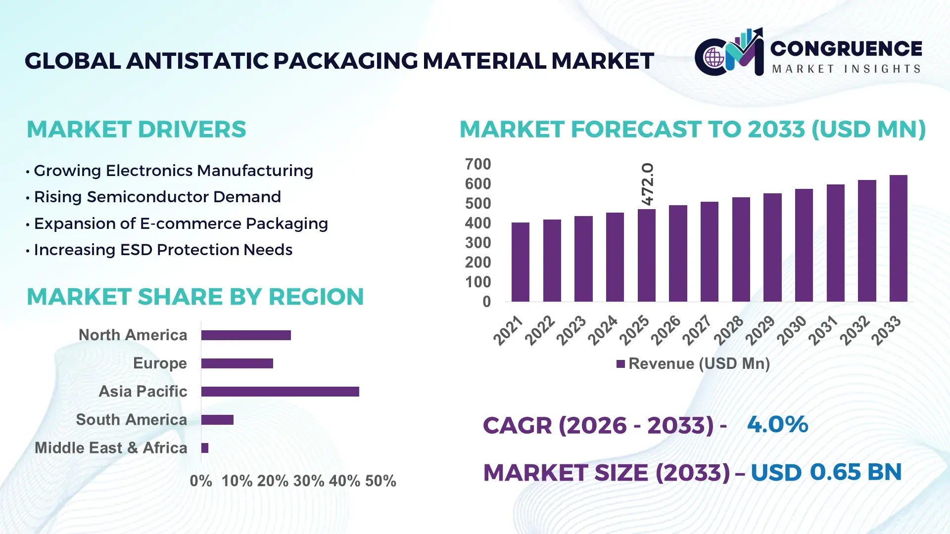
The Global Antistatic Packaging Material Market was valued at USD 472 Million in 2025 and is anticipated to reach a value of USD 645.96 Million by 2033 expanding at a CAGR of 4% between 2026 and 2033. Rising semiconductor fabrication output, electric vehicle electronics integration, and stricter electrostatic discharge protection standards across electronics manufacturing increased antistatic material adoption by over 18% in high-precision packaging applications between 2024 and 2026.
China continues to dominate the global antistatic packaging material market with nearly 38% production share, supported by electronics exports exceeding USD 3 trillion and rapid semiconductor packaging expansion across Shenzhen, Suzhou, and Chengdu. More than 62% of regional electronics manufacturers adopted upgraded ESD-safe packaging formats by 2026 to reduce component failure rates by approximately 25% compared to conventional polymer packaging. Japan and South Korea maintain strong positions through high-purity antistatic film technologies used in semiconductor wafers, lithium-ion battery cells, and precision medical electronics, while India recorded over 14% growth in localized electronics packaging demand due to expanding smartphone assembly and industrial automation investments.
Companies prioritizing localized raw material sourcing, conductive additive innovation, and automated packaging integration are strengthening resilience against regulatory pressure and global electronics supply volatility.
Market Size & Growth: USD 472 million in 2025 to USD 645.96 million by 2033 at 4% CAGR, driven by semiconductor packaging expansion and advanced electronics manufacturing growth.
Top Growth Drivers: Semiconductor packaging demand rose 19%, EV electronics integration increased 16%, and ESD compliance adoption expanded 21% globally.
Short-Term Forecast: By 2028, automated antistatic packaging lines improve handling efficiency by 24% while reducing material wastage by 17%.
Emerging Technologies: AI-based defect monitoring, multilayer conductive films, and bio-based antistatic polymers improve packaging reliability by over 22%.
Regional Leaders: Asia-Pacific exceeds USD 280 million with electronics cluster expansion, North America advances aerospace adoption, and Europe strengthens recyclable ESD packaging deployment.
Consumer/End-User Trends: Over 63% of electronics manufacturers shifted toward reusable antistatic packaging formats for high-value component transportation.
Pilot/Case Example: In 2025, a semiconductor packaging facility upgraded conductive polymer trays, reducing electrostatic damage rates by 28%.
Competitive Landscape: Top manufacturers control nearly 41% market share, led by integrated material innovators and high-volume industrial packaging suppliers.
Regulatory & ESG Impact: Recyclable antistatic material adoption increased 26% following stricter industrial waste and packaging sustainability regulations across Europe and Asia.
Investment & Funding: More than USD 1.1 billion was allocated globally toward electronics packaging expansion, conductive additive capacity, and regional manufacturing diversification.
Innovation & Future Outlook: Nanocomposite antistatic coatings and lightweight high-barrier materials accelerate next-generation electronics logistics and localized resilient supply chains.
Electronics and semiconductor applications account for nearly 52% of global antistatic packaging material consumption, followed by automotive electronics and healthcare devices with a combined 31% share. Advanced conductive films, recyclable ESD-safe polymers, and multilayer moisture-resistant packaging gained over 20% adoption growth during 2025–2026 as manufacturers focused on reducing component damage and improving compliance efficiency. Asia-Pacific continues to lead demand due to expanding chip assembly operations, while Europe accelerated sustainable packaging transitions under tightening industrial waste regulations. Increasing localization of electronics supply chains and smart packaging integration is positioning the market for more technology-focused strategic investments through the next decade.
Antistatic packaging material is rapidly transforming from a protective packaging category into a strategic infrastructure layer for global electronics, semiconductor, and EV supply chains. As component density rises and wafer-level packaging expands, manufacturers are accelerating investments in advanced ESD-safe materials that reduce product failure risks by over 27% during high-volume logistics and automated assembly operations. Global electronics localization and semiconductor reshoring initiatives are shifting procurement priorities toward regionally integrated packaging ecosystems with shorter lead cycles and higher compliance standards. Regulatory pressure surrounding recyclable industrial packaging is further forcing material innovation and supplier consolidation across Asia-Pacific, North America, and Europe.
Advanced nanocomposite antistatic films improve conductivity efficiency by 31% while reducing operational packaging costs by 18% compared to legacy polyethylene-based systems. Asia-Pacific leads in production volume with more than 46% global manufacturing concentration, while Europe leads in sustainable adoption and recyclable ESD packaging innovation with nearly 34% faster deployment across industrial electronics applications. Over the next three years, automated conductive packaging integration is projected to reduce electrostatic component rejection rates by 22% while optimizing warehouse handling throughput by 19%. Companies adopting recyclable conductive polymers are also lowering compliance-related waste management costs by approximately 16%.
In 2025, a major semiconductor exporter in Southeast Asia upgraded multilayer antistatic transport trays and improved shipment reliability by 24% across cross-border logistics operations. Global packaging manufacturers are increasingly reallocating capital toward localized conductive additive production, AI-driven defect monitoring, and high-barrier lightweight materials to secure long-term supply resilience. The competitive advantage is now shifting toward companies capable of optimizing ESD protection, sustainability compliance, and regional manufacturing responsiveness simultaneously, redefining future leadership across high-growth electronics ecosystems.
The rapid expansion of semiconductor fabrication and EV electronics manufacturing is accelerating demand for high-performance antistatic packaging materials across global supply chains. Electronics component density increased by 23% between 2024 and 2026, forcing manufacturers to adopt advanced ESD-safe packaging capable of minimizing microcircuit damage during automated handling and transportation. Simultaneously, global EV battery production capacity expanded over 28%, strengthening demand for conductive films, trays, and moisture-resistant antistatic solutions. U.S.–China technology trade restructuring pushed electronics manufacturers toward Southeast Asia and India, triggering localized packaging investments and regional supplier partnerships. In response, leading packaging companies are expanding multilayer conductive polymer capacity, accelerating automation integration, and forming strategic alliances with semiconductor assembly providers to secure long-term industrial contracts.
Volatility in conductive polymer additives and petrochemical feedstock pricing is constraining production scalability and margin stability across the antistatic packaging material market. Carbon-based conductive compound prices fluctuated nearly 18% during 2025 due to concentrated supply dependence in Asia, while industrial energy costs increased over 14% across key manufacturing hubs. Simultaneously, tightening environmental packaging regulations in Europe and North America raised compliance-related processing expenses by approximately 11%, especially for non-recyclable multilayer materials. These pressures are extending procurement cycles, delaying capacity expansion, and limiting competitiveness among mid-sized manufacturers. To mitigate risks, companies are diversifying raw material sourcing, securing long-term supplier contracts, and investing in bio-based conductive alternatives that reduce regulatory exposure while improving long-term operational flexibility and regional supply resilience.
The transition toward recyclable and lightweight conductive packaging materials is redefining growth opportunities across electronics, healthcare, and industrial automation sectors. Reusable antistatic packaging adoption increased by 26% during 2025 as manufacturers prioritized lower waste generation and reduced logistics costs. Bio-based conductive polymers demonstrated nearly 21% lower lifecycle processing expenses compared to conventional petroleum-derived materials, strengthening their strategic value in export-driven manufacturing environments. Smart packaging integration, including sensor-enabled ESD monitoring systems, improved shipment visibility and reduced handling failures by approximately 17% across high-value semiconductor logistics operations. Companies are accelerating R&D spending, expanding regional recycling ecosystems, and building vertically integrated material partnerships to capture future demand linked to sustainable electronics production, localized supply chains, and advanced industrial automation infrastructure globally.
Performance consistency across varying humidity, temperature, and transport conditions remains a major execution challenge for antistatic packaging manufacturers. Nearly 29% of electronics exporters reported higher ESD-related packaging failures during cross-border shipments involving extreme environmental exposure and extended logistics timelines. Infrastructure limitations in emerging manufacturing regions also increased fulfillment delays by 16%, constraining rapid deployment of advanced conductive packaging systems. At the same time, recyclable antistatic materials still face durability gaps of nearly 12% compared to conventional multilayer plastics in heavy industrial applications. These pressures are reshaping procurement decisions and forcing suppliers to invest aggressively in material engineering, AI-based quality monitoring, and cross-industry technology partnerships. Long-term competitiveness increasingly depends on balancing sustainability targets with high-performance reliability under global manufacturing conditions.
Reusable packaging adoption surged 26% across electronics logistics networks in 2025. Manufacturers are replacing single-use ESD materials with returnable antistatic trays and conductive containers to reduce packaging waste by 19% and lower transportation handling costs by 14%. Large electronics exporters are restructuring supplier agreements around reusable packaging cycles, while industrial packaging providers are scaling closed-loop recovery systems to optimize operational continuity under tightening sustainability regulations.
AI-driven defect monitoring reduced electrostatic packaging failures by 22% in automated facilities. Semiconductor packaging plants are integrating machine-vision inspection and sensor-enabled ESD monitoring directly into production lines, improving packaging validation speed by 18%. Labor shortages in high-volume electronics manufacturing are forcing companies to accelerate automation deployment, while packaging suppliers are expanding AI-enabled quality assurance partnerships to secure long-term manufacturing contracts.
Lightweight conductive films expanded deployment by 24% across semiconductor and PCB packaging operations. Companies are shifting from thicker multilayer plastics toward thinner nanocomposite films that reduce material consumption by 16% while maintaining conductivity stability during export logistics. This transition is reshaping procurement priorities, as packaging manufacturers optimize raw material efficiency to offset volatile polymer pricing and cross-border supply chain disruptions.
Regional manufacturing localization increased antistatic packaging conversion demand by 21% across Southeast Asia and India. Electronics assemblers are prioritizing regional sourcing partnerships to reduce shipment delays and improve inventory responsiveness by nearly 17%. A non-obvious shift is emerging where smaller regional packaging suppliers are capturing contracts previously dominated by global firms through faster customization cycles, localized compliance alignment, and flexible low-volume conductive packaging production capabilities.
The antistatic packaging material market is segmented by type, application, and end-user, with demand concentrated in high-value electronics and semiconductor protection environments. Antistatic bags and electronic component packaging collectively account for over 45% of market utilization due to scalability, low contamination risk, and compatibility with automated handling systems. Demand is rapidly shifting toward conductive foam and semiconductor protection applications as chip miniaturization increases electrostatic sensitivity. The electronics and semiconductor industries represent nearly 58% of total end-user consumption, while automotive and healthcare adoption is accelerating through advanced sensor integration and precision device manufacturing. Companies are increasingly optimizing customized ESD-safe solutions to align with regional manufacturing localization and recyclable packaging requirements.
Antistatic Bags dominate the market with approximately 34% share due to their low production cost, lightweight structure, and wide integration across electronics, PCB, and semiconductor logistics operations. Their scalability and compatibility with automated packaging systems continue strengthening structural demand across high-volume manufacturing environments. However, Conductive Foam is emerging as the fastest-growing segment, expanding by nearly 18% due to rising usage in high-fragility semiconductor wafers, EV battery electronics, and precision aerospace components requiring enhanced shock absorption and conductivity stability. The market is increasingly shifting from basic protective formats toward performance-oriented conductive solutions.
Antistatic Films and Shielding Packaging together account for nearly 38% of market demand, supported by multilayer barrier performance and increasing deployment in moisture-sensitive electronic transportation. Antistatic Trays maintain strategic relevance in reusable industrial packaging systems where durability and repetitive handling efficiency are critical. Companies are accelerating investments in recyclable conductive polymers, lightweight nanocomposite films, and customized foam structures to optimize protection efficiency while reducing logistics costs. Demand is clearly shifting toward higher-performance materials capable of balancing sustainability compliance, automation compatibility, and advanced ESD protection in complex electronics supply chains.
“According to a 2025 report by the International Electronics Manufacturing Association, conductive foam solutions were adopted by over 61% of advanced semiconductor packaging facilities, resulting in nearly 24% improvement in component protection efficiency and reduced transit-related electrostatic failures, reinforcing its growing strategic importance.”
Electronic Component Packaging leads the market with nearly 32% share due to the massive global volume of consumer electronics, industrial sensors, and communication devices requiring continuous electrostatic discharge protection throughout manufacturing and distribution cycles. Usage concentration remains strongest in automated assembly environments where lightweight, scalable, and contamination-resistant packaging formats are essential. Semiconductor Protection is the fastest-growing application, expanding by approximately 21% as advanced chip architectures and wafer miniaturization increase sensitivity to electrostatic damage during cross-border transportation and storage operations.
Consumer Electronics Packaging and PCB Packaging together contribute around 36% of total demand, supported by smartphone assembly expansion, wearable electronics growth, and high-density circuit board production. Storage and Transportation applications are gaining momentum as regional manufacturing localization forces companies to optimize shipment durability and reusable ESD-safe logistics systems. Industrial Equipment Packaging maintains strategic importance in heavy-duty electronics handling where repetitive transport cycles require stronger conductive protection layers. Companies are repositioning product portfolios toward multilayer shielding solutions, recyclable packaging structures, and AI-monitored ESD handling systems to capture rapidly evolving semiconductor and industrial automation demand patterns.
“According to a 2025 report by the Global Semiconductor Logistics Council, semiconductor protection packaging was deployed across over 4,800 electronics manufacturing facilities, improving component handling reliability by 27% and reducing electrostatic-related rejection rates by 19%, highlighting its rapid operational adoption.”
The Electronics Industry remains the dominant end-user segment with approximately 41% share due to continuous high-volume demand for ESD-safe packaging across smartphones, communication devices, industrial electronics, and consumer appliances. Strong dependency on automated assembly systems and cross-border component transportation continues driving large-scale procurement of antistatic bags, films, and shielding materials. Meanwhile, the Semiconductor Industry is the fastest-growing end-user category, recording nearly 23% expansion as advanced chip fabrication, wafer packaging, and AI hardware manufacturing intensify global electrostatic protection requirements.
Automotive and Aerospace and Defense segments are increasingly shifting toward high-performance conductive packaging due to expanding EV electronics integration, autonomous sensor systems, and mission-critical component handling requirements. Healthcare and Industrial Manufacturing collectively account for nearly 29% of market demand, supported by precision diagnostic equipment, industrial automation devices, and sensitive instrumentation logistics. Buying behavior is evolving toward customized recyclable packaging systems, long-term supply agreements, and localized sourcing partnerships. Companies are strategically targeting these sectors through specialized conductive material development, region-specific packaging customization, and integrated ESD monitoring capabilities to capture future high-value industrial demand.
“According to a 2025 report by the Advanced Electronics Packaging Consortium, adoption among semiconductor industry manufacturers increased by 28%, with over 3,200 facilities implementing advanced conductive packaging systems, leading to nearly 22% improvement in production reliability and handling efficiency, indicating a strong shift in demand dynamics.”
Asia-Pacific accounted for the largest market share at 46% in 2025 however, North America is expected to register the fastest growth, expanding at a CAGR of 5.2% between 2026 and 2033.
Asia-Pacific dominates global antistatic packaging material production due to large-scale electronics manufacturing concentration across China, South Korea, Japan, and India, with over 58% of semiconductor packaging demand linked to regional supply chains. North America is accelerating through semiconductor reshoring initiatives, advanced EV electronics production, and automated ESD-safe logistics adoption, while Europe leads sustainable conductive packaging innovation with nearly 34% recyclable material integration across industrial electronics applications. Supply chain diversification following U.S.–China trade restructuring is shifting regional sourcing strategies and forcing manufacturers to localize packaging operations for faster delivery cycles and compliance alignment. Global companies are increasingly prioritizing Asia-Pacific for scale, North America for high-value technology integration, and Europe for sustainability-driven product innovation and regulatory positioning.
North America holds approximately 24% of global antistatic packaging material demand, supported by semiconductor manufacturing expansion, aerospace electronics production, and EV battery component logistics. The U.S. dominates regional consumption as semiconductor reshoring initiatives and electronics supply chain localization accelerate procurement of advanced ESD-safe materials. Automated conductive packaging adoption increased by nearly 22% across high-volume manufacturing facilities during 2025, improving handling efficiency and reducing electrostatic rejection rates. Companies are expanding AI-enabled inspection systems and recyclable conductive packaging deployment to comply with stricter industrial sustainability targets. More than 31% of electronics manufacturers shifted toward localized packaging suppliers to reduce import dependency and shipment delays. Businesses are prioritizing this region for technology-intensive packaging innovation, high-margin industrial demand, and supply chain resilience.
Europe accounts for nearly 21% of global antistatic packaging material consumption, driven by industrial electronics manufacturing, automotive sensor integration, and medical device packaging demand across Germany, France, and the Netherlands. Strict environmental packaging regulations are reshaping procurement strategies, with recyclable conductive material adoption increasing by approximately 29% during 2025. Enterprises are prioritizing lightweight multilayer shielding solutions that reduce industrial waste generation by nearly 17% while maintaining high ESD protection standards. Regional manufacturers are accelerating investments in bio-based conductive polymers and closed-loop packaging recovery systems to strengthen compliance efficiency and export competitiveness. Quality-first purchasing behavior remains dominant, especially among semiconductor and automotive electronics suppliers seeking long-term regulatory alignment. This region is forcing companies to innovate faster around sustainable packaging performance and circular material integration.
Asia-Pacific leads the global antistatic packaging material market with nearly 46% demand concentration, supported by massive electronics, semiconductor, and consumer device manufacturing capacity across China, Japan, South Korea, and India. China alone contributes over 38% of regional conductive packaging output due to integrated electronics supply chains and export-oriented industrial infrastructure. Localized packaging production expanded by approximately 27% during 2025 as manufacturers optimized delivery speed and reduced dependence on imported ESD-safe materials. High-volume electronics assemblers are rapidly adopting lightweight conductive films and reusable trays to improve logistics efficiency and reduce packaging losses by nearly 18%. Enterprises across the region prioritize cost scalability, production speed, and supply continuity, making Asia-Pacific the critical operational center for global packaging expansion and manufacturing partnerships.
South America contributes nearly 6% of global antistatic packaging material demand, with Brazil and Argentina leading regional consumption through automotive electronics assembly, industrial manufacturing, and localized appliance production. Infrastructure limitations and imported conductive material dependency increased packaging procurement costs by approximately 15% during 2025, constraining rapid scalability across smaller manufacturing sectors. However, regional electronics packaging demand expanded by over 13% as companies accelerated local sourcing strategies to reduce shipment delays and currency-related import exposure. Manufacturers are increasingly deploying reusable antistatic trays and low-cost conductive films for industrial logistics optimization. Price-sensitive buyers continue prioritizing durable, scalable packaging formats over premium multilayer solutions. The region presents a high-potential expansion opportunity, but operational success depends on cost control, localized partnerships, and supply chain adaptability.
The Middle East & Africa region accounts for nearly 5% of global antistatic packaging material demand, supported by industrial automation investments, electronics imports, and expanding aerospace and energy infrastructure projects across the UAE, Saudi Arabia, and South Africa. Industrial equipment packaging demand increased by approximately 16% during 2025 as regional modernization programs accelerated deployment of sensitive electronic control systems. Strategic partnerships between packaging suppliers and industrial manufacturers are improving localized conductive material availability and reducing logistics lead times by nearly 12%. Enterprises increasingly prefer durable antistatic trays and shielding packaging capable of handling extreme transportation and storage conditions. Investment-led infrastructure transformation and industrial diversification are positioning the region as an emerging strategic market for specialized high-performance protective packaging solutions.
China – 38% market share in the Antistatic Packaging Material market due to massive electronics manufacturing capacity, integrated semiconductor supply chains, and large-scale export-driven packaging demand.
United States – 21% market share in the Antistatic Packaging Material market supported by semiconductor reshoring, advanced aerospace electronics production, and strong adoption of automated ESD-safe packaging technologies.
The antistatic packaging material market is dominated by global material innovators competing directly with regional cost-focused manufacturers and specialized ESD packaging suppliers. Top players including Desco Industries, Dou Yee Enterprises, Kureha Corporation, Miller Packaging, and Protective Packaging Corporation collectively control nearly 43% of market activity through advanced conductive materials, customized industrial solutions, and long-term electronics manufacturing partnerships. Competition is increasingly centered on recyclable conductive polymers, multilayer shielding performance, and supply chain responsiveness, with automated packaging integration improving operational efficiency by approximately 21%. Regional suppliers are competing aggressively on pricing and localized delivery speed, while global leaders are accelerating vertical integration, semiconductor-focused product development, and production expansion across Asia-Pacific and North America. Material innovation cycles shortened nearly 18% during 2025 due to rising semiconductor packaging complexity. High-performance reliability, compliance-ready sustainable materials, and scalable regional manufacturing networks now define the core barriers to competitive market entry.
Desco Industries Inc.
Dou Yee Enterprises
Kureha Corporation
Miller Packaging
Protective Packaging Corporation
Smurfit Kappa Group
Sealed Air Corporation
Teknis Limited
Botron Company Inc.
GWP Group
Elcom UK
Selen Science & Technology Co. Ltd.
Polyplus Packaging
Conductive Containers Inc.
Advanced conductive polymer technologies are currently dominating antistatic packaging operations as electronics manufacturers prioritize higher ESD protection accuracy and automated logistics compatibility. Multilayer conductive films improved electrostatic discharge resistance efficiency by nearly 28% compared to conventional polyethylene packaging while reducing product handling failures by 19% across semiconductor transportation systems. More than 61% of high-volume electronics facilities adopted automated ESD-safe packaging integration by 2026 to optimize throughput speed and reduce manual inspection dependency. Companies deploying lightweight shielding films and reusable conductive trays are lowering logistics waste while strengthening shipment reliability in high-fragility component environments.
Emerging technologies are reshaping material engineering through nanocomposite coatings, AI-driven defect monitoring, and bio-based conductive polymers. AI-enabled inspection systems reduced packaging validation time by approximately 21%, while nanocomposite antistatic films lowered raw material consumption by nearly 16% without compromising conductivity stability. Recyclable conductive packaging adoption crossed 34% across Europe and North America as manufacturers accelerated compliance-focused packaging transformation. Companies integrating smart ESD sensors into semiconductor logistics systems are gaining operational advantages through real-time monitoring and lower rejection risks.
Disruptive packaging innovation between 2026 and 2028 is centered on self-regulating conductive materials and digitally traceable packaging ecosystems. Advanced nanocomposite packaging improves conductivity consistency by 31% while reducing lifecycle operational costs by 18% compared to legacy static shielding systems. Semiconductor exporters, EV battery manufacturers, and aerospace electronics suppliers are accelerating partnerships with material innovators to secure high-performance packaging capacity. Competitive leadership is increasingly shifting toward companies capable of combining sustainability compliance, AI-driven quality control, and localized advanced material production simultaneously.
May 2025 – Desco Industries introduced VpCI-125 HP Bags combining corrosion inhibition and permanent static dissipative protection for sensitive electronics and aerospace components. The bags achieved surface resistance below 1.0 x 10¹¹ ohms, improving electrostatic protection stability during long-duration storage and export logistics operations. [Dual-Protection Upgrade] Source: Desco Blog
April 2026 – Sealed Air Corporation expanded deployment of recyclable Korrvu retention packaging for electronics and EV charger transportation, integrating anti-static protective films with recyclable corrugated structures containing up to 50% recycled material. The solution reduced inbound storage space requirements while strengthening reusable packaging efficiency. [Recyclable ESD Shift] Source: Sealed Air
August 2025 – Schütz Container Systems announced a USD 31 million expansion of its Missouri industrial packaging facility, adding a new manufacturing line focused on advanced protective packaging formats. The investment strengthened localized North American packaging production and improved regional delivery responsiveness for industrial electronics customers. [Localized Capacity Push] Source:
November 2025 – Sealed Air Corporation accelerated automation-focused packaging operations after reporting a 4.2% increase in adjusted EBITDA linked to operational optimization and high-performance packaging integration. The company expanded automation and protective packaging deployment across electronics logistics and industrial fulfillment environments to improve throughput consistency. [Automation Efficiency Drive] Source: SECWatch Reddit Feed
The Antistatic Packaging Material Market Report delivers comprehensive coverage across material types, applications, end-user industries, regional demand structures, and emerging conductive packaging technologies. The analysis evaluates Antistatic Bags, Conductive Foam, Antistatic Films, Shielding Packaging, and reusable tray systems across electronic component packaging, semiconductor protection, PCB transportation, industrial equipment handling, and consumer electronics logistics. The report covers five major geographic regions and profiles leading manufacturing countries shaping global conductive packaging supply chains. More than 58% of evaluated demand patterns are linked to electronics and semiconductor applications, while recyclable conductive packaging adoption surpassed 34% across advanced industrial markets.
The report provides deep operational and strategic analysis covering supply chain localization, AI-enabled defect monitoring, nanocomposite conductive materials, and sustainable ESD-safe packaging integration trends between 2026 and 2033. It assesses over 12 major industry participants, regional production shifts, deployment intensity, and packaging conversion trends influencing competitive positioning. Strategic insights highlight where manufacturers are accelerating capacity expansion, automation integration, and recyclable material investments to improve shipment reliability, regulatory alignment, and logistics efficiency. The scope also captures emerging niche opportunities including sensor-enabled smart packaging systems and lightweight conductive barrier technologies reshaping advanced electronics transportation and semiconductor logistics ecosystems.
| Report Attribute/Metric | Report Details |
|---|---|
|
Market Revenue in 2025 |
USD 472 Million |
|
Market Revenue in 2033 |
USD 645.96 Million |
|
CAGR (2026 - 2033) |
4% |
|
Base Year |
2025 |
|
Forecast Period |
2026 - 2033 |
|
Historic Period |
2021 - 2025 |
|
Segments Covered |
By Type
By Application
By End-User
|
|
Key Report Deliverable |
Revenue Forecast, Growth Trends, Market Dynamics, Segmental Overview, Regional and Country-wise Analysis, Competition Landscape |
|
Region Covered |
North America, Europe, Asia-Pacific, South America, Middle East, Africa |
|
Key Players Analyzed |
Desco Industries Inc., Dou Yee Enterprises, Kureha Corporation, Miller Packaging, Protective Packaging Corporation, Smurfit Kappa Group, Sealed Air Corporation, Teknis Limited, Botron Company Inc., GWP Group, Elcom UK, Selen Science & Technology Co. Ltd., Polyplus Packaging, Conductive Containers Inc. |
|
Customization & Pricing |
Available on Request (10% Customization is Free) |


