
Reports
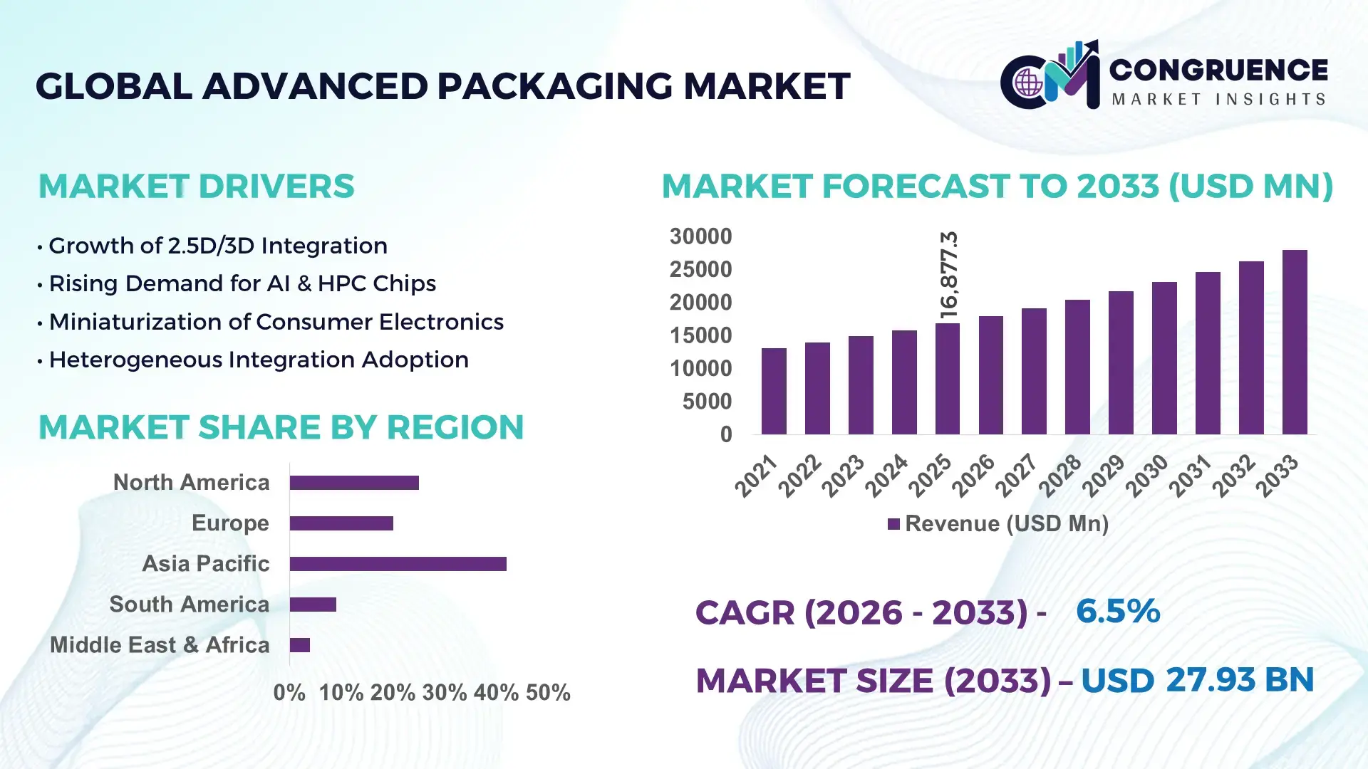
The Global Advanced Packaging Market was valued at USD 16,877.26 Million in 2025 and is anticipated to reach a value of USD 27,931.8 Million by 2033, expanding at a CAGR of 6.5% between 2026 and 2033, driven by growing demand for miniaturized and high-performance semiconductor devices.
The United States dominates the Advanced Packaging market, with over 120 production facilities specializing in wafer-level and 3D packaging solutions. In 2025, investments exceeded USD 2.3 billion in next-generation packaging technologies such as heterogeneous integration and fan-out wafer-level packaging (FOWLP). Key applications include high-performance computing, automotive electronics, and 5G devices. Adoption of chiplet-based solutions grew by 40% year-on-year, while more than 65% of semiconductor OEMs integrated advanced packaging in their product lines. Strong R&D efforts focus on reducing latency, increasing density, and improving energy efficiency.
Market Size & Growth: USD 16,877.26 Million in 2025 to USD 27,931.8 Million by 2033 at 6.5% CAGR, driven by high-performance semiconductor demand.
Top Growth Drivers: Miniaturization adoption 45%, Performance improvement 38%, Power efficiency enhancement 30%.
Short-Term Forecast: By 2028, packaging cycle times expected to reduce by 25%, throughput to improve by 20%.
Emerging Technologies: 3D ICs, Fan-Out Wafer-Level Packaging (FOWLP), Chiplet integration.
Regional Leaders: USA USD 9,200M (2033) with high HPC adoption, China USD 6,500M (2033) with consumer electronics growth, Taiwan USD 5,100M (2033) with foundry-driven innovations.
Consumer/End-User Trends: Increased adoption in automotive, mobile, HPC, and IoT devices; preference for energy-efficient, compact electronics.
Pilot or Case Example: 2024 pilot of FOWLP in automotive ICs reduced package size by 35% and improved thermal performance by 22%.
Competitive Landscape: Market leader: Intel (~18%), competitors: TSMC, ASE Technology, Amkor, SPIL.
Regulatory & ESG Impact: Compliance with RoHS, REACH, and semiconductor environmental standards; incentives for green packaging technologies.
Investment & Funding Patterns: USD 3.2B invested in 2025 across new fab expansions, venture-backed packaging startups, and R&D programs.
Innovation & Future Outlook: Focus on heterogeneous integration, wafer-level fan-out solutions, AI-driven design automation, and eco-friendly materials.
The Advanced Packaging Market is being reshaped by high-growth sectors such as automotive electronics, 5G devices, HPC, and consumer electronics. Innovations like 3D IC stacking, fan-out wafer-level packaging, and chiplet integration are enhancing performance, miniaturization, and energy efficiency. Regional production capacities, supportive policies, and ESG-driven initiatives are accelerating adoption. Emerging trends indicate AI-assisted design, high-density packaging, and sustainable materials will define the next wave of market growth, ensuring strong long-term expansion.
The Advanced Packaging Market holds strategic importance as semiconductor manufacturers increasingly prioritize miniaturization, heterogeneous integration, and high-performance computing solutions. Fan-Out Wafer-Level Packaging (FOWLP) delivers up to 30% improvement in thermal efficiency compared to traditional wire-bond packaging, enabling high-density, low-latency electronics. Asia-Pacific dominates in volume, while North America leads in adoption with over 65% of semiconductor OEMs implementing advanced packaging solutions. By 2028, AI-driven design optimization is expected to improve packaging throughput by 20%, reducing design cycle times and accelerating time-to-market. Firms are committing to ESG improvements such as 25% reduction in electronic waste through recyclable packaging materials by 2030, aligning production with sustainable manufacturing initiatives.
Micro-scenarios demonstrate measurable impact: in 2025, Intel’s integration of 3D IC stacking achieved a 22% increase in thermal dissipation efficiency, enhancing high-performance computing outputs. Strategic pathways for the market include expansion into automotive electronics, 5G devices, and IoT systems, with a focus on integrating AI-assisted design tools and energy-efficient materials. Forward-looking projections suggest the Advanced Packaging Market will remain a pillar of resilience, compliance, and sustainable growth, providing scalable, high-performance semiconductor solutions while meeting global environmental and regulatory standards.
The growing need for compact, energy-efficient, and high-performance electronic devices has significantly accelerated the adoption of advanced packaging solutions. Miniaturization enables the integration of multiple chips in a single package, reducing board space by up to 40% while maintaining high-speed performance. Applications in automotive electronics, 5G smartphones, HPC servers, and IoT devices are driving demand for fan-out wafer-level packaging (FOWLP) and 3D IC stacking. Semiconductor OEMs are implementing these solutions to enhance thermal management, reduce latency, and improve signal integrity, with over 60% of high-end consumer electronics adopting advanced packaging techniques by 2025. This trend underscores the market’s strategic relevance, positioning it as a critical enabler for next-generation electronics innovation.
Advanced packaging solutions require significant capital investment in fabrication facilities, specialized equipment, and skilled labor. The production of 3D ICs and FOWLP involves multiple processing steps such as wafer thinning, die stacking, and redistribution layer formation, which increase operational complexity. Initial setup costs can exceed USD 150 million per new fab line, limiting entry for smaller manufacturers. Additionally, precise alignment and thermal management requirements create yield challenges, with some facilities experiencing up to 10% scrap rates during initial runs. Variability in global material supply chains and compliance with stringent environmental regulations further complicate manufacturing, restraining the speed of adoption despite high market demand.
The rapid growth of electric vehicles, autonomous driving systems, and 5G-enabled devices provides significant opportunities for advanced packaging adoption. Automotive ICs increasingly require high-density, thermally efficient packages, with FOWLP reducing package size by 35% and improving reliability under extreme temperature conditions. In 5G infrastructure, high-bandwidth modules demand heterogeneous integration for low-latency signal transmission. Semiconductor manufacturers can leverage this demand to expand production capabilities, invest in AI-assisted design tools, and develop next-generation packaging materials. By integrating AI and automation in production lines, companies can improve throughput by 20–25% while reducing defect rates, opening untapped market potential across high-growth technology sectors.
The Advanced Packaging Market faces challenges from rising equipment costs, labor-intensive processes, and evolving regulatory requirements. Maintaining quality and yield in 3D IC stacking and wafer-level packaging is technically demanding, requiring precision machinery and expert operators. Compliance with RoHS, REACH, and semiconductor environmental standards increases operational overheads, particularly for recycled and eco-friendly materials. Additionally, supply chain volatility for high-purity silicon, specialty resins, and advanced substrates introduces delays and cost fluctuations. Firms also face competitive pressure to innovate rapidly while ensuring energy efficiency, thermal performance, and reliability. These combined factors create barriers to scaling production and achieving cost-effective, high-volume output across regions.
Surge in 3D IC Integration: The adoption of 3D IC stacking continues to accelerate, with over 48% of high-performance computing and server modules implementing vertical integration in 2025. This trend allows for a 30–35% increase in transistor density per package and improves signal transmission speeds by up to 25%. Asia-Pacific leads in production volume, while North America sees adoption in over 60% of AI and HPC applications. Thermal management innovations in 3D ICs have reduced operating temperatures by an average of 15%, enhancing device reliability.
Expansion of Fan-Out Wafer-Level Packaging (FOWLP): FOWLP adoption has grown rapidly, with 42% of smartphone and 5G ICs incorporating this technology by 2025. This method decreases package size by approximately 35% while improving interconnect density and performance. Demand for advanced inspection and precision lithography tools has risen by 28%, particularly in Taiwan and South Korea, where high-volume production meets stringent miniaturization requirements. FOWLP has also enabled a 20% improvement in thermal dissipation compared to conventional flip-chip solutions.
AI-Driven Packaging Design and Automation: AI-assisted design tools now influence over 50% of advanced packaging layouts, cutting design cycle time by 22% and reducing material wastage by 18%. Predictive analytics optimize die placement, signal routing, and thermal management for high-density packages. North America leads in AI adoption, with 65% of semiconductor fabs integrating AI-driven optimization, while Europe focuses on automating assembly lines for high-precision packaging. This trend ensures faster time-to-market and consistent quality for complex multi-die systems.
Sustainable and Eco-Friendly Packaging Materials: Companies are increasingly adopting recyclable substrates and low-impact resins, with over 38% of advanced packaging fabs committing to 20–25% material recycling by 2025. These efforts reduce electronic waste while meeting ESG compliance requirements. Europe leads in sustainable material adoption, whereas North America focuses on energy-efficient process integration, achieving up to 15% reduction in energy consumption per package. The focus on sustainability also drives innovations in bio-based polymers and water-soluble underfill materials.
The Advanced Packaging Market is segmented across product types, application areas, and end-users, each offering distinct insights into adoption patterns and growth potential. By type, the market encompasses fan-out wafer-level packaging, 3D ICs, system-in-package (SiP), and flip-chip technologies, each designed to optimize performance, density, and thermal efficiency. Applications span high-performance computing, automotive electronics, consumer electronics, and telecommunications, with varying adoption trends driven by device miniaturization and energy efficiency requirements. End-user insights highlight semiconductor manufacturers, OEMs, and electronics integrators as primary adopters, with regional differences in production scale, technology penetration, and investment priorities shaping market dynamics. The segmentation analysis provides decision-makers with an understanding of technology preferences, adoption trends, and strategic pathways for targeted growth initiatives.
Fan-out wafer-level packaging (FOWLP) currently leads the Advanced Packaging market, accounting for 38% of adoption, driven by its ability to reduce package size by up to 35% while improving thermal performance and interconnect density. 3D IC integration is the fastest-growing type, projected to see a 7.2% growth in adoption due to increasing demand in high-performance computing and AI-enabled devices for vertical chip stacking and enhanced signal integrity. System-in-package (SiP) solutions contribute around 20% of the market, offering multi-die integration for IoT and automotive applications, while traditional flip-chip packages account for the remaining 15%, mainly in legacy consumer electronics and industrial modules.
High-performance computing (HPC) represents the leading application segment, accounting for 40% of adoption, due to the need for high-density, low-latency packages in data centers, AI servers, and cloud computing infrastructure. Automotive electronics is the fastest-growing application, expected to see 6.8% adoption growth, driven by EVs and autonomous vehicle systems requiring thermally stable and compact packaging. Consumer electronics, including smartphones and wearables, make up 25% of the market, while telecommunications modules represent 15%, focusing on 5G and high-bandwidth connectivity.
Semiconductor manufacturers are the dominant end-users, representing 45% of the market, integrating advanced packaging solutions into high-performance computing, automotive, and 5G device production. OEMs in consumer electronics are the fastest-growing end-user segment, with adoption expected to rise 7% due to demand for compact, energy-efficient devices in smartphones, tablets, and smart wearables. Electronics integrators and industrial system providers account for 25% of the remaining market, focusing on IoT modules, networking devices, and specialized industrial applications.
Asia-Pacific accounted for the largest market share at 42% in 2025, however, North America is expected to register the fastest growth, expanding at a CAGR of 6.8% between 2026 and 2033.
Asia-Pacific leads in production volume with over 120 advanced packaging fabrication units, producing more than 1.5 billion packaged ICs annually. China contributes approximately 55% of regional consumption, followed by Japan at 22% and India at 15%. Advanced packaging adoption in high-performance computing, automotive electronics, and mobile AI applications is driving regional demand. North America, with 38% adoption in 2025, emphasizes high-tech integration and AI-driven optimization in semiconductor fabs. Europe accounts for 12% of market share, with regulatory pressure for sustainable and explainable packaging solutions shaping adoption. South America and the Middle East & Africa together contribute 8% of the global market, largely supported by telecom infrastructure upgrades, energy projects, and industrial electronics. Across regions, consumer behavior varies, with APAC focusing on mobile and e-commerce electronics, North America on enterprise computing, and Europe on compliance-driven adoption.
How are technological advancements and enterprise adoption shaping the market?
North America holds 38% of the Advanced Packaging market, driven by semiconductor fabs in the U.S. and Canada. Key industries include high-performance computing, automotive electronics, and AI-driven devices. Government incentives for semiconductor innovation and updated environmental regulations have accelerated adoption of sustainable packaging practices. Digital transformation trends such as AI-assisted design, automated assembly, and predictive thermal management are increasingly prevalent. Intel and AMD are actively implementing 3D IC stacking and fan-out wafer-level packaging in server processors and automotive chips. Regional consumer behavior shows higher enterprise adoption in healthcare and finance sectors, with over 60% of major corporations integrating advanced packaging in AI and HPC systems, emphasizing miniaturization, energy efficiency, and performance optimization.
What drives adoption in compliance-focused technology sectors?
Europe accounts for 12% of the Advanced Packaging market, with Germany, France, and the UK as leading contributors. Regulatory bodies enforce RoHS and REACH compliance, prompting manufacturers to adopt eco-friendly materials and explainable packaging solutions. Key industries include automotive electronics, aerospace, and industrial automation. Adoption of 3D ICs and FOWLP is increasing, particularly in high-precision manufacturing hubs like Germany’s Baden-Württemberg region. Local players, such as STMicroelectronics, are implementing fan-out packaging for automotive and industrial modules, enhancing device reliability and reducing package size by 30%. European enterprises prioritize regulatory alignment, with 55% of packaging projects integrating ESG metrics and traceable material usage, reflecting a compliance-driven market behavior.
Why does manufacturing scale and innovation hub development drive growth?
Asia-Pacific leads with 42% of the global Advanced Packaging market in 2025. Top consuming countries include China (55%), Japan (22%), and India (15%). Regional infrastructure emphasizes high-volume semiconductor fabs, with more than 120 advanced packaging units producing over 1.5 billion packaged ICs annually. Technology trends include chiplet integration, 3D IC stacking, and fan-out wafer-level packaging. Local players, such as ASE Technology and TSMC, are pioneering FOWLP and heterogeneous integration for HPC, mobile, and automotive devices. Consumer behavior is driven by mobile AI applications, e-commerce electronics, and high-performance computing adoption, with over 65% of device manufacturers integrating advanced packaging in new product lines to optimize density, thermal efficiency, and power consumption.
How are infrastructure and local incentives influencing market adoption?
South America holds approximately 4% of the global Advanced Packaging market, with Brazil and Argentina as key contributors. The market is influenced by energy infrastructure projects, telecom network upgrades, and industrial automation. Government incentives, including tax reductions and trade agreements, encourage semiconductor assembly and packaging investments. Local players focus on modular packaging solutions for industrial electronics and telecom devices, improving reliability and reducing cycle time by 15%. Regional consumer behavior shows demand driven by media, language localization, and enterprise adoption in industrial and telecom sectors, with Brazil accounting for over 60% of regional advanced packaging integration.
What role do modernization and strategic investments play in market growth?
The Middle East & Africa represent 4% of the global Advanced Packaging market, with UAE and South Africa leading adoption. Regional demand is driven by oil & gas electronics, telecom infrastructure, and industrial automation. Technological modernization includes AI-assisted assembly lines and predictive thermal management systems. Local regulations and trade partnerships encourage sustainable packaging practices and import of high-precision components. Key local players are adopting fan-out wafer-level packaging in telecommunications and industrial applications. Consumer behavior reflects enterprise-focused adoption, particularly in energy, construction, and telecom, with 55% of installations in critical infrastructure projects incorporating advanced packaging to optimize reliability and performance.
China – 28% market share; dominant due to high production capacity, large-scale semiconductor manufacturing, and strong domestic demand for consumer electronics.
United States – 25% market share; strong end-user demand in HPC, automotive, and AI applications, supported by regulatory incentives and investment in advanced packaging R&D.
The Advanced Packaging market is moderately consolidated, with around 150 active competitors globally, including semiconductor foundries, system-in-package specialists, and assembly service providers. The top 5 companies, including Intel, TSMC, ASE Technology, Amkor, and SPIL, collectively account for approximately 58% of the global market share, reflecting a concentration of high-volume production capacity and technological leadership. Competitive positioning focuses on high-performance computing, automotive electronics, 5G devices, and consumer electronics, with firms differentiating through innovative packaging technologies such as 3D IC stacking, fan-out wafer-level packaging, and heterogeneous integration.
Strategic initiatives have intensified, including joint ventures, R&D partnerships, and targeted acquisitions. For example, companies are investing in AI-assisted design tools, thermal optimization solutions, and wafer-level reliability testing to improve package density and performance. Product launches are increasingly focused on miniaturization, high-density interconnects, and energy-efficient packaging. Innovation trends, including chiplet integration and environmentally sustainable materials, are reshaping the competitive landscape, compelling players to scale manufacturing while reducing lead times and enhancing package yield. North America and Asia-Pacific remain critical competitive hubs, hosting over 70% of advanced packaging production units, while Europe emphasizes compliance-driven innovation.
Amkor Technology
SPIL (Siliconware Precision Industries)
AMD
Samsung Electronics
STMicroelectronics
Qualcomm
Texas Instruments
Micron Technology
NXP Semiconductors
GlobalFoundries
Infineon Technologies
Marvell Technology
The Advanced Packaging market is being shaped by both current and emerging technologies that enhance performance, density, and energy efficiency in semiconductor devices. Fan-Out Wafer-Level Packaging (FOWLP) remains a leading technology, implemented in over 42% of smartphone and 5G ICs in 2025, enabling package size reduction by up to 35% and improving interconnect density by 28%. 3D IC stacking is rapidly gaining traction, with 48% of high-performance computing modules incorporating vertical die integration, resulting in 30% faster signal transmission and a 15% reduction in operating temperature. System-in-Package (SiP) solutions are widely adopted in automotive and IoT applications, representing 20% of current advanced packaging deployments, providing multi-die integration in compact form factors.
Emerging technologies are further redefining the market landscape. Chiplet-based architectures allow modular design of processors, with over 60% of AI and HPC servers adopting chiplet integration to improve scalability and reduce latency. AI-assisted design automation tools are being deployed in more than 50% of semiconductor fabs in North America, optimizing die placement, thermal management, and signal integrity while reducing design cycle times by 22% and material waste by 18%. High-density interposers and embedded passive components are increasingly used to support heterogeneous integration across multiple dies.
Sustainability-driven innovations, including bio-based substrates, water-soluble underfill, and recyclable packaging materials, are being integrated in over 38% of advanced packaging facilities, addressing ESG objectives and reducing electronic waste. Collectively, these technologies are enabling miniaturization, higher performance, and energy-efficient semiconductor solutions, positioning the Advanced Packaging market as a critical enabler for next-generation electronics across HPC, automotive, 5G, and consumer electronics sectors.
• In February 2025, ASMPT SEMI Solutions unveiled its next‑generation wire bonder with X‑POWER 2.0 technology, engineered to enhance semiconductor manufacturing efficiency and precision for high‑density packaging applications, addressing demand in AI and automotive electronics sectors. (Semi)
• In March 2025, ASMPT introduced the CamSpector PRO automated optical inspection system with advanced 2D and 3D wire bond inspection capabilities, improving detection accuracy down to 0.7 µm and increasing production throughput by more than 20% for image sensor packaging. (ASMPT)
• In February 2025, ASE Technology Holding Co. projected that its advanced packaging and testing revenue would more than double to approximately $1.6 billion in 2025, up from $600 million in 2024, driven by escalating global demand for AI chips and leading‑edge packaging services. (Reuters)
• In October 2025, Amkor Technology commenced groundbreaking on a new high‑volume advanced packaging and test campus in Arizona, expanding total investment to $7 billion with additional cleanroom space and facilities designed to strengthen U.S. semiconductor back‑end capabilities. (Amkor Marketing External)
The scope of the Advanced Packaging Market Report encompasses a comprehensive analysis of technologies, segments, geographic regions, and industry applications shaping advanced semiconductor packaging. It covers major packaging types including fan‑out wafer‑level packaging, system‑in‑package (SiP), 3D IC stacking, flip‑chip, and emerging formats such as heterogeneous integration and chiplet‑based architectures, detailing unit shipments, substrate usage, and interconnect density metrics across each type. Regional insights span North America, Europe, Asia‑Pacific, South America, and Middle East & Africa, examining production capacities, fab expansions, policy impacts, and adoption trends in key consumer and industrial markets. Application focus areas include high‑performance computing, automotive electronics, 5G infrastructure, IoT modules, and consumer devices, with data on adoption percentages and integration complexities relevant to decision‑makers. The report also explores end‑user segments such as semiconductor manufacturers, OEMs, and contract assembly & test providers, including detailed analyses of technology requirements and unit demands. Innovation trends such as AI‑assisted packaging design, high‑density interposers, hybrid bonding techniques, and sustainability‑oriented materials are addressed, alongside competitive dynamics, patent activity, and strategic collaboration models. Emerging and niche segments such as photonics packaging and bio‑compatible materials are also examined, ensuring a full picture of market evolution and strategic pathways.
| Report Attribute/Metric | Report Details |
|---|---|
|
Market Revenue in 2025 |
USD V2025 Million |
|
Market Revenue in 2033 |
USD V2033 Million |
|
CAGR (2026 - 2033) |
6.5% |
|
Base Year |
2025 |
|
Forecast Period |
2026 - 2033 |
|
Historic Period |
2021 - 2025 |
|
Segments Covered |
By Types
By Application
By End-User
|
|
Key Report Deliverable |
Revenue Forecast, Growth Trends, Market Dynamics, Segmental Overview, Regional and Country-wise Analysis, Competition Landscape |
|
Region Covered |
North America, Europe, Asia-Pacific, South America, Middle East, Africa |
|
Key Players Analyzed |
|
|
Customization & Pricing |
Available on Request (10% Customization is Free) |


