
Reports
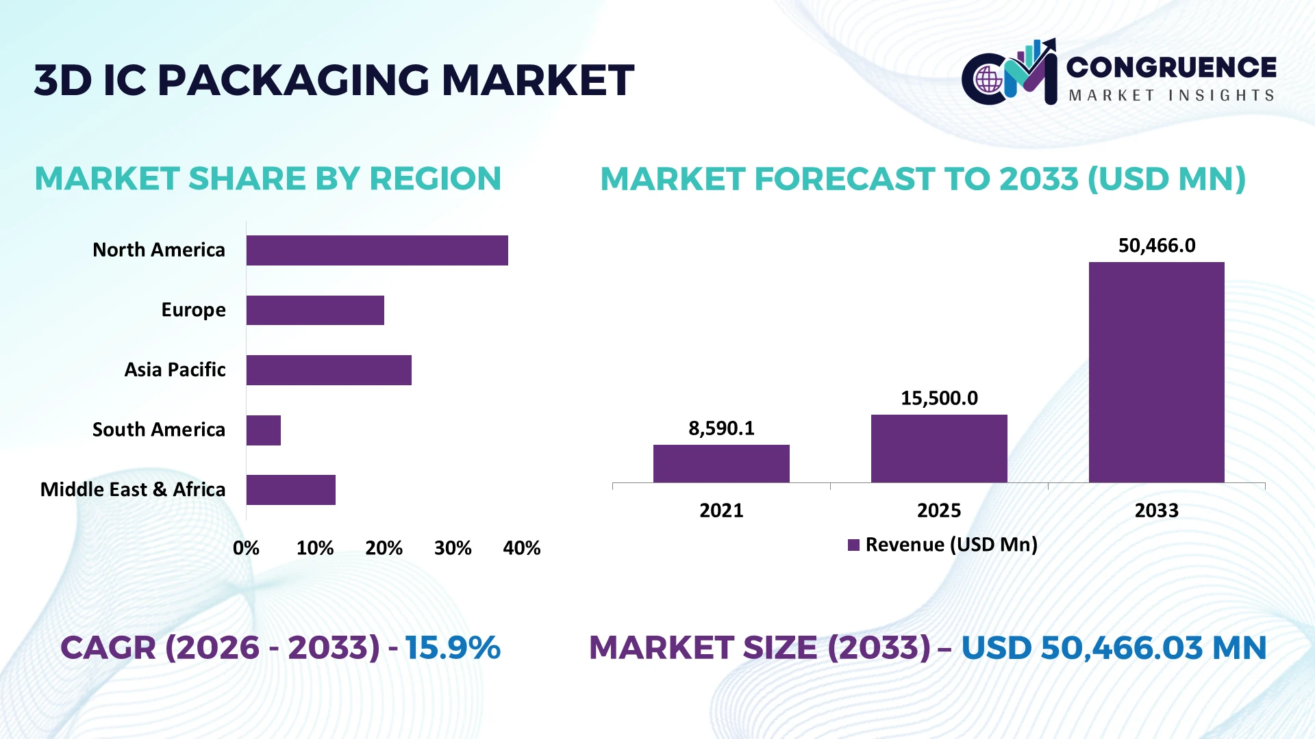
The Global 3D IC Packaging Market was valued at USD 15500 Million in 2025 and is anticipated to reach a value of USD 50466.03 Million by 2033 expanding at a CAGR of 15.9% between 2026 and 2033. AI accelerators, HBM integration, chiplet architectures, and tighter logic-memory interconnects are driving adoption of TSVs, hybrid bonding, silicon interposers, and advanced wafer-level packaging.
Taiwan dominates advanced packaging capacity, with TSMC targeting roughly 130,000 CoWoS wafers monthly by end-2026 as AI-chip demand intensifies; Taiwan also manufactures over 60% of global foundry output. South Korea leads HBM manufacturing through SK hynix and Samsung, while the U.S. is adding domestic advanced-packaging capacity under CHIPS Act incentives amid semiconductor supply-chain localization and U.S.–China technology restrictions.
Strategically, semiconductor companies must secure HBM, hybrid-bonding, substrate, and advanced-packaging capacity early because packaging capability increasingly determines AI accelerator performance and shipment scalability.
Market Size & Growth: USD 15.5 billion in 2025 reaches USD 50.47 billion by 2033 at 15.9%, driven by AI accelerators and HBM integration.
Top Growth Drivers: AI-server shipments rise 28%, HBM bit demand exceeds 50% growth, while advanced-node complexity increases packaging intensity above 20%.
Short-Term Forecast: By 2028, hybrid bonding targets sub-10-micron interconnect pitches, delivering over 30% higher interconnect density versus conventional micro-bump architectures.
Emerging Technologies: Sub-10-micron hybrid bonding, TSV stacking, glass substrates, and backside power delivery are redefining high-density 3D integration.
Regional Leaders: By 2033, indicative shares imply Asia-Pacific USD 31.3 billion, North America USD 10.1 billion, and Europe USD 5.6 billion as advanced packaging localizes.
End-User Trends: Data-center AI accelerators increasingly integrate 6–12 HBM stacks, sharply increasing demand for interposers, TSVs, and thermal-management technologies.
Pilot/Case Example: Intel’s 2025 Clearwater Forest architecture combines 12 compute chiplets using 3D Foveros packaging, increasing core density while separating process technologies.
Competitive Landscape: TSMC commands roughly 35% of advanced packaging activity; ASE, Amkor, Intel, Samsung, and JCET compete through capacity and heterogeneous integration.
Regulatory & ESG Impact: U.S. CHIPS incentives exceed USD 52 billion, accelerating domestic semiconductor manufacturing and advanced-packaging supply-chain localization.
Investment & Funding: TSMC’s U.S. investment plan totals USD 165 billion, including advanced packaging and R&D infrastructure supporting AI semiconductor localization.
Innovation & Future Outlook: Hybrid bonding below 5-micron pitch and 16+ HBM-die stacks will shift competition from transistor scaling toward system-level integration.
The 3D IC Packaging Market is becoming critical to AI accelerators, high-performance computing, smartphones, networking silicon, and HBM-intensive data centers. Advanced hybrid bonding and chiplet integration are pushing interconnect pitches below 10 microns, improving bandwidth density while reducing communication distance. U.S.–China technology restrictions and semiconductor localization are simultaneously reshaping capacity decisions, making packaging availability a strategic consideration for the next phase of industry competition.
3D IC packaging is becoming strategically decisive as AI accelerators, high-bandwidth memory, and chiplet architectures shift semiconductor competition from transistor scaling toward system-level integration. Supply chains are simultaneously restructuring: the U.S. targets at least three high-volume advanced-packaging facilities by 2030, while Taiwan and South Korea retain deeper manufacturing ecosystems. This localization is redirecting packaging investment toward domestic capacity, substrates, testing, and thermal management.
Hybrid bonding provides a clear performance step beyond conventional micro-bump stacking. Intel’s Foveros Direct uses sub-5-micron copper-to-copper interconnects, compared with 36-micron micro-bumps in Foveros 2.5D, enabling substantially denser die-to-die connectivity and lower resistance. By 2028, advanced platforms are targeting more than 24 interconnected dies and over 38 bridge connections per package.
Operationally, Intel already combines 3D stacking with EMIB architectures for packages exceeding 100 billion transistors and 47 active tiles. Companies are therefore expanding hybrid-bonding lines, HBM partnerships, known-good-die testing, and advanced substrate capacity. Between 2026 and 2028, competitive advantage will increasingly belong to suppliers that control design enablement, packaging yield, thermal performance, and scalable heterogeneous integration.
AI infrastructure is forcing packaging density higher because compute, HBM, and specialized I/O increasingly exceed the practical limits of monolithic dies. Intel projects advanced EMIB configurations moving from roughly 8 interconnected dies in 2023 to more than 12 in 2026 and over 24 by 2028, while bridge counts rise beyond 20 and 38 respectively. SK hynix began HBM4 mass shipments in 2026 and secured multi-year agreements with around 10 major customers, confirming structural demand for vertically integrated memory systems. Chipmakers are responding through hybrid-bonding investment, substrate expansion, and packaging-design co-optimization. The strategic insight is that AI-system shipment capacity increasingly depends on packaging throughput, not simply wafer availability.
3D architectures multiply manufacturing dependencies because one defective die, bonding interface, or TSV layer can impair an entire high-value package. Conventional Foveros implementations still use approximately 36-micron micro-bump pitch, while next-generation hybrid bonding compresses interconnects below 5 microns, sharply tightening alignment and process-control tolerances. Intel consequently emphasizes known-good-die screening and system-level testing to prevent defective components from advancing into costly final assemblies. Supply concentration compounds the constraint: advanced substrates, HBM, packaging equipment, and specialty materials remain clustered in Asian manufacturing ecosystems. Companies are reducing exposure through multi-sourcing, domestic capacity, long-term supply contracts, and pre-bond testing. The strongest operational lever is yield protection before stacking, where defect avoidance preserves package economics.
Hybrid bonding creates a major opportunity to combine logic, memory, accelerators, and I/O using process nodes optimized for each function rather than fabricating every component monolithically. Intel’s Foveros Direct supports sub-5-micron copper-to-copper pitch, versus 36 microns for its earlier Foveros 2.5D interface, while research pathways target more than 10-fold interconnect-density improvement. U.S. policy also supports commercialization: federal programs committed $300 million specifically to advanced-packaging research and up to $1.6 billion toward areas including chiplets, power delivery, and thermal management. Suppliers are building open chiplet ecosystems, advanced test capability, and design partnerships. The non-obvious opportunity lies in mixing mature and leading-edge dies, lowering unnecessary advanced-node usage while improving system customization.
As packages move toward vertically stacked compute and memory, power density, warpage, thermal gradients, and die-to-die interoperability become harder to control. Intel’s scaling roadmap shows package dimensions expanding from roughly 80×80 mm in 2023 toward about 120×120 mm in 2026 and beyond 120×180 mm by 2028, while integrated die counts exceed 24. Larger, denser assemblies increase cooling complexity and magnify the consequences of interface failure. At the same time, interoperable chiplets require common electrical, test, and packaging standards across foundries and suppliers. Intel already works with more than 40 ecosystem partners across seven alliances, illustrating the coordination burden. Companies must invest in thermal engineering, standardized interfaces, advanced inspection, digital twins, and collaborative design ecosystems to sustain reliable high-volume deployment.
HBM Stacks Reshape Package Design: HBM4 entered mass shipment in 2026 with bandwidth doubled versus the prior generation and power efficiency improved by more than 40%. SK hynix also shipped 12-layer HBM4E samples delivering 16Gbps per pin and over 20% higher power efficiency. Packaging suppliers are expanding TSV, thermal-interface, and high-density interconnect capability to support AI accelerators with increasingly memory-centric architectures.
Hybrid Bonding Moves Toward Production: Intel is advancing Foveros Direct with interconnect pitches below 5 µm, materially denser than roughly 36 µm micro-bump implementations. This transition reduces interconnect distance, parasitic resistance, and latency while enabling finer die partitioning. Foundries and OSAT providers are scaling copper-to-copper bonding, surface preparation, metrology, and known-good-die workflows to protect yield as 3D stack complexity rises.
Packaging Supply Chains Localize: U.S. advanced-packaging capacity is broadening as export controls and CHIPS-driven localization reduce reliance on concentrated Asian supply. Intel processed the first wafer through Fab 52 in Arizona and is adding outsourced advanced-packaging capacity in Korea during 2026. Suppliers are restructuring sourcing, qualification, and customer support around geographically diversified assembly and test networks.
Chiplet Ecosystems Become More Open: UCIe adoption and heterogeneous integration are changing package design from proprietary stacking toward interoperable chiplet architectures. Intel’s 2026 AI platforms combine Foveros Direct 3D, UCIe-S, HBM, and up to 256 cores. The non-obvious shift is commercial: packaging vendors increasingly compete on ecosystem compatibility, design enablement, and integration services rather than assembly capability alone.
3D TSV leads the specified technology mix with approximately 38% share in 2025, reflecting its established role in HBM, vertically interconnected memory, image sensors, and logic-memory integration. Its mature process ecosystem across etching, copper filling, wafer thinning, and stacking provides greater production scalability than newer approaches. 3D Die Stacking and 3D Wafer Stacking remain important for memory and compact system architectures, benefiting from proven vertical integration but facing tighter yield economics as stack heights increase. Approximately 58% of TSV production is associated with 300 mm substrates, underscoring the technology’s dependence on high-volume wafer infrastructure.
3D Hybrid Bonding is the fastest-shifting segment as AI processors require higher interconnect density and reduced bump pitch. Sub-10 µm bonding is replacing conventional micro-bump interfaces in leading-edge designs, while Intel’s Foveros Direct targets below 5 µm. 3D Foveros remains strategically smaller but increasingly important for heterogeneous compute. Companies are consequently directing capital toward hybrid-bonding equipment, surface activation, metrology, and die-to-wafer processes, shifting investment from mature interconnect scaling toward direct copper connectivity.
High-Performance Computing represents the largest specified application, with HPC and AI together accounting for about 37–47% of 3D IC packaging demand in 2025 depending on scope. HPC remains dominant because processors require high-bandwidth memory, large interposers, chiplet integration, and dense die-to-die connectivity to overcome reticle and memory-bandwidth limits. Memory Devices form another substantial demand pool; HBM alone represents roughly 40% of device-level 3D packaging activity in one 2025 assessment. Networking & Communications maintains strategic relevance as switches, optical interconnects, and high-speed processors adopt heterogeneous packaging to reduce latency and power loss.
Artificial Intelligence is the fastest-expanding application as accelerator designs add larger HBM stacks and custom compute chiplets. SK hynix’s HBM4 delivers more than 2× bandwidth over the previous generation, while HBM4E reaches 16Gbps per pin. Consumer Electronics remains more mature, emphasizing compactness and power efficiency rather than maximum package density. Suppliers are reallocating CoWoS, TSV, hybrid-bonding, and substrate capacity toward AI and HPC customers, where performance requirements justify higher packaging complexity and tighter supplier integration.
OSAT Providers represent the largest end-user group within advanced packaging operations, accounting for approximately 59% of the broader semiconductor advanced-packaging structure in 2025, while foundry and integrated-manufacturer activity represented about 39%. ASE, Amkor, and JCET benefit from established assembly, substrate handling, final test, and customer qualification networks, giving OSATs scale advantages across diversified semiconductor programs. Foundries are nevertheless increasing direct control of premium 3D platforms through CoWoS, SoIC, Foveros, and related heterogeneous-integration services. Semiconductor Manufacturers remain major users where memory and logic suppliers vertically integrate packaging with device design.
Data Center Operators are the fastest-shifting end-user group because hyperscale AI infrastructure increasingly determines package configuration upstream. Hyperscalers and cloud providers represented approximately 73% of AI-accelerator 2.5D/3D packaging demand in 2025. Electronics OEMs remain more diversified, emphasizing power, form factor, and unit economics. Packaging companies are therefore building direct engineering relationships with hyperscalers, expanding reserved capacity, and offering customized chiplet, HBM, and thermal solutions rather than relying solely on conventional semiconductor procurement channels.
Asia-Pacific accounted for the largest market share at 62% in 2025 however, North America is expected to register the fastest growth, expanding at a CAGR of 16.8% between 2026 and 2033.
Domestic Advanced Packaging Capacity Accelerates
North America represents approximately 20% of 3D IC packaging demand, anchored by AI accelerators, high-performance computing, data centers, and semiconductor supply-chain localization. The U.S. is shifting from heavy dependence on Asian back-end capacity toward domestic heterogeneous integration under CHIPS-driven manufacturing policy. Intel’s Arizona operations provide Foveros and EMIB capabilities, while Amkor is developing a major Arizona advanced packaging and test facility targeting high-performance computing and communications chips. TSMC is also adding advanced packaging capability alongside its expanded U.S. manufacturing footprint. This infrastructure buildout connects leading-edge wafers with domestic assembly, testing, and chiplet integration, reducing logistics exposure for strategic semiconductors. Cloud operators including Microsoft, Google, Meta, and Amazon further concentrate demand for HBM-intensive accelerators, making packaging capacity increasingly important to U.S. AI infrastructure deployment.
U.S. Market Outlook: The United States combines hyperscale AI demand, advanced processor design, semiconductor equipment expertise, and expanding domestic manufacturing. Intel’s Foveros Direct targets sub-5-micron interconnect pitch, enabling substantially denser chiplet connectivity than conventional micro-bump packaging. Arizona is becoming a critical packaging corridor as foundries, OSAT providers, equipment suppliers, and semiconductor designers co-locate advanced manufacturing capabilities.
Chiplet Research Bridges Manufacturing Gaps
Europe accounts for approximately 11% of global 3D IC packaging activity, with demand concentrated around automotive semiconductors, industrial electronics, telecommunications, high-performance computing, and research-intensive heterogeneous integration. Germany, France, Belgium, the Netherlands, and Ireland anchor semiconductor design and manufacturing ecosystems, while imec provides globally significant R&D capability in hybrid bonding and wafer-level integration. The European Chips Act targets a 20% global semiconductor production share by 2030, strengthening investment in pilot lines, advanced nodes, packaging, and chiplet technologies. Europe remains less vertically integrated in high-volume advanced packaging than Taiwan or South Korea, making research-to-production transfer strategically important. Companies are responding through collaborative pilot lines and cross-border semiconductor ecosystems. Automotive electrification provides a differentiated demand base, particularly for high-reliability packaging where thermal performance and lifecycle durability matter more than maximum AI-compute density.
Germany Market Outlook: Germany provides Europe’s strongest industrial demand base through automotive, power electronics, factory automation, and semiconductor manufacturing. Dresden’s semiconductor cluster includes GlobalFoundries, Infineon, Bosch-linked supply chains, and expanding European capacity. Advanced packaging investment increasingly targets automotive processors and heterogeneous modules requiring higher reliability, thermal stability, and qualification standards than mainstream consumer semiconductor packages.
Integrated Supply Chains Preserve Scale Advantage
Asia-Pacific controls approximately 62% of the 3D IC packaging market, reflecting unparalleled concentration across foundries, HBM manufacturing, OSAT services, substrates, assembly equipment, and semiconductor materials. Taiwan anchors high-end logic packaging through TSMC’s CoWoS and SoIC platforms, while South Korea dominates HBM supply through SK hynix and Samsung. China adds substantial OSAT scale through JCET and Tongfu Microelectronics, and Japan remains critical in substrates, bonding materials, chemicals, and precision equipment. TSMC continues expanding CoWoS capacity as NVIDIA and other accelerator designers require larger logic-plus-HBM packages. This geographically dense supplier network shortens qualification cycles and supports rapid volume ramping. U.S.–China technology controls are simultaneously accelerating localized Chinese packaging investment, creating a more segmented Asian ecosystem in which supply-chain security increasingly influences equipment selection and customer allocation.
Taiwan Market Outlook: Taiwan is the most strategically important national hub because TSMC combines leading-edge wafer fabrication with CoWoS, InFO, and SoIC integration. The country accounts for more than 60% of global foundry output, while expanding CoWoS capacity addresses AI accelerator bottlenecks. Its dense substrate, testing, equipment, and assembly ecosystem gives customers shorter development-to-volume-production pathways.
Brazil Builds Back-End Semiconductor Capability
South America represents approximately 2% of global 3D IC packaging activity, with Brazil accounting for the majority of meaningful semiconductor assembly, design, and electronics demand. The region lacks the high-volume TSV, hybrid-bonding, HBM, and advanced substrate infrastructure established in East Asia, making imported components essential for servers, telecommunications equipment, automotive electronics, and industrial systems. Brazil’s semiconductor policy renewal and Nova Indústria Brasil framework are strengthening incentives for domestic chip design, assembly, and electronics manufacturing. Existing back-end capabilities provide a foundation for progressively higher-value packaging, although equipment availability, wafer supply, engineering talent, and ecosystem depth remain limiting factors. Companies are therefore emphasizing partnerships, technology transfer, design services, and incremental packaging modernization rather than immediate leading-edge 3D capacity. The strongest near-term positioning lies in specialized industrial and automotive packages linked to Brazil’s large electronics-consuming industries.
Brazil Market Outlook: Brazil combines South America’s largest electronics manufacturing base with semiconductor design capabilities and established back-end operations. São Paulo and southern industrial clusters support automotive, telecommunications, industrial, and consumer-electronics demand. Government semiconductor incentives increasingly emphasize domestic design and manufacturing resilience, creating opportunities for packaging modernization, workforce development, and international technology partnerships rather than direct competition with Asian mega-fabs.
Semiconductor Investment Creates New Capacity Nodes
Middle East & Africa contributes approximately 5% of global 3D IC packaging demand, led increasingly by Gulf investment in AI infrastructure, data centers, sovereign technology programs, and semiconductor ecosystem development. Saudi Arabia and the UAE are building compute-intensive digital economies, increasing downstream demand for HBM-equipped accelerators and advanced packaged processors even before substantial local packaging production emerges. Israel contributes established semiconductor design, fabrication, and advanced computing expertise, while Morocco and South Africa maintain electronics and automotive manufacturing capabilities. Saudi Arabia’s National Semiconductor Hub targets 50 semiconductor design companies by 2030, demonstrating a deliberate shift toward higher-value technology localization. Rather than immediately replicating Taiwan’s manufacturing depth, Gulf economies are using investment funds, international partnerships, data-center demand, and design incentives to establish ecosystem entry points. Packaging opportunities initially center on design enablement, testing, system integration, and specialized assembly.
Saudi Arabia Market Outlook: Saudi Arabia is positioning semiconductors within its broader technology localization strategy, supported by the National Semiconductor Hub and rapidly expanding AI infrastructure. Its target of attracting 50 semiconductor design companies creates a future customer base for advanced packaging services. Strategic capital, data-center expansion, and international technology partnerships provide a pathway from chip design toward localized assembly, testing, and heterogeneous integration.
TSMC, ASE Technology, Amkor, Intel, Samsung, and JCET compete across overlapping advanced-packaging layers, with foundry-integrated leaders challenging OSAT specialists through tighter wafer-to-package control. The top five suppliers hold approximately 55–60% of advanced 3D packaging activity. TSMC differentiates through CoWoS and SoIC, while Intel pushes sub-5-micron Foveros Direct; OSAT leaders counter through broader customer access, customization, and outsourced scale. Hybrid bonding delivers over 80% interconnect-pitch reduction versus 36-micron micro-bumps, while HBM4 improves power efficiency above 40%, shifting competition toward thermal and electrical performance. Players are expanding capacity, securing substrate and HBM partnerships, and vertically integrating testing with assembly. Supply concentration in Taiwan and South Korea is accelerating U.S., European, and Chinese localization. High equipment costs, yield control, known-good-die testing, and customer qualification remain formidable entry barriers. Winning requires protected capacity, sub-10-micron integration, high yields, supply-chain resilience, and deep design-to-manufacturing collaboration across global customer programs.
TSMC
ASE Technology Holding Co., Ltd.
Amkor Technology, Inc.
Intel Corporation
Samsung Electronics Co., Ltd.
JCET Group Co., Ltd.
SK hynix Inc.
Micron Technology, Inc.
United Microelectronics Corporation
Powertech Technology Inc.
Tongfu Microelectronics Co., Ltd.
ChipMOS Technologies Inc.
Unisem (M) Berhad
Nepes Corporation
Current 3D IC packaging is centered on TSVs, micro-bumps, silicon interposers, and HBM integration for AI and HPC processors. TSMC’s 3nm SoIC entered volume production in 2025, while advanced packaging interconnect density has doubled since 2023. Dense vertical connections reduce data movement, improving bandwidth efficiency and strengthening accelerator performance.
Emerging hybrid bonding replaces solder micro-bumps with direct copper connections. Intel’s Foveros Direct targets below 5-micron pitch versus roughly 36 microns for conventional Foveros micro-bumps, an interconnect-pitch reduction exceeding 86%. Sub-10-micron die-to-wafer hybrid bonding is already in production. Foundries, OSATs, and memory suppliers benefit through higher I/O density, lower resistance, and tighter logic-memory integration.
Disruptive architectures combine chiplets, HBM4, co-packaged optics, backside power, and intelligent packaging-fab automation. HBM4 doubles bandwidth and improves power efficiency by over 40% versus HBM3E, while TSMC uses deep learning and image recognition in packaging operations. Through 2026–2028, 3D packaging will shift toward larger heterogeneous systems, finer-pitch bonding, and optical I/O as advanced capacity approaches 1.4 million wafers monthly. Companies controlling bonding yield, thermal engineering, substrates, and integrated testing gain the strongest competitive advantage. Acting now secures qualification experience and scarce production capacity before AI architectures require even denser system integration across next-generation data-center compute platforms globally.
October 2024 — Amkor Technology and TSMC signed an Arizona advanced-packaging agreement covering InFO and CoWoS services. Proximity between Phoenix wafer fabrication and Peoria back-end operations targets shorter product cycle times and stronger U.S. semiconductor supply resilience capacity. Source: amkor.com
July 2025 — Applied Materials highlighted fine-pitch die-to-wafer hybrid bonding at SEMI’s Advanced Packaging Summit, where sub-10-micron D2W bonding was identified as already in production. The transition improves I/O density, power performance, and thermal management for 3DIC systems. Source: semi.org
September 2025 — SK hynix completed HBM4 development and prepared mass production, delivering double HBM3E bandwidth and over 40% better power efficiency. The 12-layer architecture strengthens vertically stacked memory performance for next-generation AI accelerators and data centers systems. Source: skhynix.com
April 2026 — TSMC confirmed plans for an Arizona advanced-packaging facility operational before 2029, addressing a critical U.S. AI-chip bottleneck. Domestic CoWoS and 3D-IC capability will reduce dependence on shipping Arizona-fabricated wafers back to Taiwan for packaging operations. Source: reuters.com
The 3D IC Packaging Market report evaluates 3D TSV, 3D Wafer Stacking, 3D Hybrid Bonding, 3D Die Stacking, and 3D Foveros across High-Performance Computing, Artificial Intelligence, Memory Devices, Consumer Electronics, and Networking & Communications. End-user analysis covers semiconductor manufacturers, foundries, OSAT providers, electronics OEMs, and data-center operators, alongside North America, Europe, Asia-Pacific, South America, and Middle East & Africa.
Technology coverage includes sub-10-micron hybrid bonding, TSV integration, chiplets, HBM4, silicon interposers, co-packaged optics, advanced thermal management, and automated packaging fabs. Asia-Pacific accounts for approximately 62% of market activity, while hybrid-bonding interconnect pitches are moving below 5 microns and advanced packaging capacity is projected toward 1.4 million wafers monthly by 2028. The 2026–2033 assessment supports capacity investment, supplier qualification, geographic expansion, technology partnerships, competitive benchmarking, and strategic positioning as packaging becomes increasingly decisive to semiconductor system performance.
| Report Attribute/Metric | Report Details |
|---|---|
Market Revenue in 2025 | USD 15500 Million |
Market Revenue in 2033 | USD 50466.03 Million |
CAGR (2026 - 2033) | 15.9% |
Base Year | 2025 |
Forecast Period | 2026 - 2033 |
Historic Period | 2021 - 2025 |
Segments Covered | By Type
By Application
By End-User
|
Key Report Deliverable | Revenue Forecast, Growth Trends, Market Dynamics, Segmental Overview, Regional and Country-wise Analysis, Competition Landscape |
Region Covered | North America, Europe, Asia-Pacific, South America, Middle East, Africa |
Key Players Analyzed | TSMC, ASE Technology Holding Co., Ltd., Amkor Technology, Inc., Intel Corporation, Samsung Electronics Co., Ltd., JCET Group Co., Ltd., SK hynix Inc., Micron Technology, Inc., United Microelectronics Corporation, Powertech Technology Inc., Tongfu Microelectronics Co., Ltd., ChipMOS Technologies Inc., Unisem (M) Berhad, Nepes Corporation |
Customization & Pricing | Available on Request (10% Customization is Free) |