
Reports
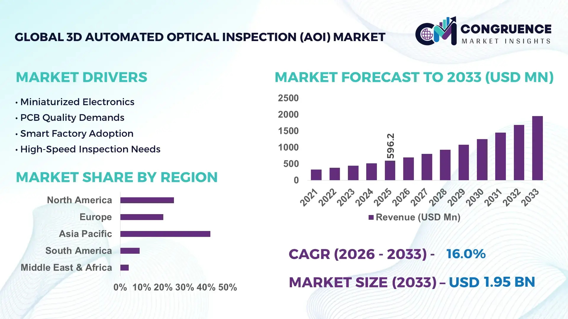
The Global 3D Automated Optical Inspection (AOI) Market was valued at USD 596.23 Million in 2025 and is anticipated to reach a value of USD 1954.7 Million by 2033 expanding at a CAGR of 16% between 2026 and 2033, driven by rising demand for high-precision quality control in electronics manufacturing.
Japan leads the 3D Automated Optical Inspection (AOI) market, with its production capacity exceeding 1,200 units annually across major electronics manufacturing hubs. Investments in advanced inspection robotics reached approximately USD 320 Million in 2025, targeting semiconductor, PCB, and automotive electronics sectors. Key industry applications include defect detection in multilayer PCBs, solder joint inspection, and component verification. Japan’s technology landscape emphasizes high-speed 3D imaging and AI-enabled inspection algorithms, with adoption rates above 70% in high-volume production facilities. Regional distribution shows strong deployment in Kansai and Kanto areas, with top-tier manufacturers integrating AOI systems into smart factory initiatives.
Market Size & Growth: Valued at USD 596.23 Million in 2025, projected to reach USD 1954.7 Million by 2033, CAGR of 16% due to precision manufacturing demand.
Top Growth Drivers: PCB defect detection adoption 68%, automotive electronics inspection efficiency 55%, semiconductor inspection automation 60%.
Short-Term Forecast: By 2028, defect detection accuracy expected to improve by 25%, reducing rework costs.
Emerging Technologies: AI-driven inspection algorithms, 3D X-ray integrated AOI, high-speed optical sensors.
Regional Leaders: Japan USD 620 Million, South Korea USD 480 Million, Germany USD 350 Million by 2033, highlighting advanced robotics adoption.
Consumer/End-User Trends: Electronics manufacturers increasingly integrating AOI for inline quality control, especially in automotive and semiconductor sectors.
Pilot or Case Example: 2025 pilot in Osaka semiconductor plant achieved 30% reduction in production downtime.
Competitive Landscape: Market leader: Omron (~18%), major competitors: Nordson DAGE, Koh Young, CyberOptics, ViTrox.
Regulatory & ESG Impact: Compliance with IPC standards, incentives for smart factory automation, ESG focus on reducing manufacturing waste.
Investment & Funding Patterns: USD 320 Million invested in AOI R&D and system upgrades, strong venture funding for AI-enabled inspection tech.
Innovation & Future Outlook: Growing integration of AI, machine learning, and 3D X-ray systems; expansion into automotive EV electronics and high-density PCBs.
The 3D Automated Optical Inspection (AOI) market is witnessing rapid innovation across electronics, automotive, and semiconductor sectors. Recent product developments include AI-enhanced defect recognition and multi-angle 3D imaging capabilities, improving inspection speed and accuracy. Regulatory compliance with IPC and environmental standards is driving adoption in high-volume production. Regional consumption is strongest in East Asia, with rising interest in Europe for automotive electronics. Future trends indicate integration with Industry 4.0 smart factory initiatives, predictive maintenance analytics, and scalable inspection solutions for next-generation PCBs and semiconductor components.
The 3D Automated Optical Inspection (AOI) Market holds strategic relevance as a cornerstone for precision, compliance, and operational efficiency in electronics and semiconductor manufacturing. Advanced AI-enabled AOI systems deliver up to 35% improvement in defect detection compared to traditional 2D optical inspection methods, ensuring higher throughput and lower rework costs. Japan dominates in volume, while South Korea leads in adoption with over 72% of enterprises integrating AOI into their production lines. By 2028, predictive maintenance AI algorithms are expected to reduce unplanned downtime by 28%, enhancing overall equipment efficiency. Firms are committing to ESG improvements such as a 20% reduction in manufacturing waste and enhanced recycling of PCB scrap by 2030. In 2025, a pilot initiative at a major Japanese semiconductor plant achieved a 30% reduction in soldering defects through AI-enhanced 3D AOI implementation. Strategic investment in multi-angle 3D imaging and high-speed optical sensors positions manufacturers to meet stringent quality standards while supporting sustainable growth. Looking forward, the 3D Automated Optical Inspection (AOI) Market is projected to remain a pillar of resilience, compliance, and innovation-driven expansion across global electronics and automotive manufacturing sectors.
The growing complexity of multilayer PCBs and high-performance semiconductors is driving demand for 3D AOI systems capable of detecting micro-defects with high precision. With production lines increasingly automated, manufacturers are leveraging AI-based 3D AOI to identify solder joint failures, missing components, and micro-cracks that are undetectable by traditional methods. In 2025, over 70% of semiconductor assembly plants in East Asia integrated advanced AOI systems, reducing defect-related downtime by 25%. The technology’s ability to support inline inspection for high-density interconnects and complex automotive electronics positions it as a critical tool for ensuring consistent product quality and minimizing costly rework. Investments in multi-angle imaging and faster optical sensors are further accelerating adoption.
Despite the benefits, the 3D AOI market faces challenges due to significant capital expenditures and integration complexity. High-precision inspection systems often require investments exceeding USD 200,000 per unit, including installation and calibration costs. Small and medium-sized manufacturers may face budgetary constraints, delaying adoption. Integration with existing production lines requires specialized technical expertise, leading to extended setup times and potential workflow disruptions. Additionally, training operators to interpret AI-driven inspection outputs and maintaining consistent accuracy in high-speed production lines presents operational hurdles. Compliance with industry standards such as IPC also adds complexity, as frequent updates necessitate continuous system adjustments. These factors collectively slow market penetration, particularly in regions with smaller electronics manufacturing bases.
The rapid expansion of electric vehicles (EVs) and high-density electronics offers significant growth potential for the 3D AOI market. Advanced battery management systems, high-density PCBs, and power electronics demand precise defect detection and quality control. In 2025, over 60% of automotive electronics manufacturers in Japan and South Korea began adopting 3D AOI to ensure reliability and reduce recalls. Emerging trends, such as AI-enhanced predictive defect detection and integration with Industry 4.0 smart factories, provide measurable improvements in production yield and defect reduction. Additionally, new applications in consumer electronics and wearable devices, which require miniaturized yet highly reliable components, are driving demand for sophisticated inspection systems capable of meeting tight tolerances.
Operational costs, including maintenance, software updates, and energy consumption, present a significant challenge for AOI system operators. Advanced 3D AOI systems require periodic recalibration, sensor upgrades, and AI model retraining to maintain accuracy, increasing total cost of ownership. Compliance with strict IPC and ISO standards necessitates continuous monitoring, documentation, and process validation, adding to operational complexity. Furthermore, variations in regional regulations, such as environmental disposal rules for PCB waste, require adaptive system configurations. These challenges, combined with the need for skilled operators and integration with multi-vendor production lines, can limit adoption rates, particularly among smaller manufacturers or those with legacy systems in place. Operational disruptions and regulatory non-compliance risks make careful planning and investment in scalable AOI solutions critical for long-term success.
Surge in AI-Enabled Defect Detection: The integration of AI algorithms in 3D AOI systems is transforming quality assurance processes. Over 68% of high-volume electronics manufacturers have implemented AI-driven inspection tools, resulting in an average 30% reduction in false defect identification and a 25% faster inspection cycle. AI-enabled systems now allow predictive identification of potential failures, enhancing throughput in semiconductor and automotive electronics production lines.
Expansion of Multi-Angle 3D Imaging: Multi-angle inspection technology adoption has grown by 60% among PCB and semiconductor producers to address complex board structures. Systems now capture up to 360-degree component views, enabling detection of micro-cracks and soldering defects that were previously undetectable. High-density interconnects and layered PCBs are increasingly requiring these advanced imaging solutions, particularly in East Asia and Western Europe, where precision manufacturing standards are stringent.
Integration with Smart Factory Initiatives: Over 70% of manufacturing plants in Japan and South Korea have connected AOI systems to Industry 4.0 networks, enabling real-time data analytics and automated corrective actions. This connectivity has led to a 20% reduction in production downtime and a 15% improvement in overall equipment effectiveness (OEE). Remote monitoring and predictive maintenance applications are driving operational efficiency and lowering inspection bottlenecks.
Adoption in Electric Vehicle and High-Density Electronics Manufacturing: The rise of EVs and compact consumer electronics has driven AOI adoption by 58% among relevant manufacturers. These systems are now essential for battery management modules, power electronics, and miniature PCB assemblies, achieving up to 35% higher defect detection rates compared to conventional inspection. Regions like North America lead in adoption, while East Asia dominates in deployment volume, highlighting the global expansion of AOI applications.
The 3D Automated Optical Inspection (AOI) market is segmented by type, application, and end-user, offering targeted insights for strategic decision-making. By type, systems vary from single-lens 3D AOI to multi-angle and laser-assisted models, each optimized for specific inspection requirements. Application segmentation includes PCB inspection, semiconductor defect detection, automotive electronics, and other high-precision manufacturing use cases, reflecting the diverse deployment of AOI technologies. End-user segmentation highlights electronics manufacturers, automotive OEMs, semiconductor fabs, and contract manufacturing services, with adoption patterns influenced by production volume, defect tolerance, and quality compliance standards. Regional preferences also influence segmentation, with East Asia leading in volume deployment and Europe emphasizing regulatory compliance and precision-driven adoption. Overall, segmentation analysis underscores how technological capabilities, application-specific demands, and end-user priorities collectively shape market evolution and investment strategies.
Among the various types of 3D AOI systems, multi-angle AOI leads the market, accounting for 48% of adoption due to its superior ability to inspect high-density and multilayer PCBs with complex layouts. Single-lens 3D AOI currently holds 32% of the market, providing cost-effective solutions for less complex assembly lines. Laser-assisted AOI is emerging fastest, expected to surpass 25% adoption by 2033, driven by its precision in detecting micro-cracks and solder joint defects on miniaturized components. Other niche types, including inline hybrid AOI systems and automated X-ray integrated AOI, contribute a combined 20% share, serving specialized applications such as semiconductor packaging and automotive electronics.
PCB inspection dominates the 3D AOI market, representing 50% of adoption due to increasing PCB complexity and multilayer designs. Semiconductor defect detection accounts for 30% of applications, providing precise evaluation of solder joints, die alignment, and wafer packaging. The fastest-growing application is automotive electronics inspection, projected to surpass 22% adoption by 2033, driven by high integration of sensors, EV power modules, and safety-critical electronic systems. Other applications, including consumer electronics, aerospace components, and medical device inspection, represent a combined 18% share, where precision and regulatory compliance are essential.
Electronics manufacturers are the leading end-users of 3D AOI systems, accounting for 55% of adoption, driven by inline quality monitoring and defect reduction in high-volume production lines. Semiconductor fabs are the fastest-growing end-user segment, expected to exceed 25% adoption by 2033, fueled by the increasing complexity of ICs and advanced packaging requirements. Automotive OEMs and contract manufacturers collectively represent a 20% share, leveraging AOI systems to ensure component reliability and compliance with safety standards. In East Asia, over 70% of high-volume electronics production facilities employ multi-angle 3D AOI for PCB and semiconductor inspection, while North American automotive plants report a 65% adoption rate for inline electronic module inspection.
Asia-Pacific accounted for the largest market share at 42% in 2025; however, North America is expected to register the fastest growth, expanding at a CAGR of 14% between 2026 and 2033.
Asia-Pacific’s dominance is driven by high-volume electronics manufacturing in China, Japan, and South Korea, with over 1,500 3D AOI systems deployed in 2025 across PCB and semiconductor production lines. North America’s growth is fueled by automotive electronics and semiconductor fabs, with more than 65% of manufacturers integrating advanced AOI solutions. Europe follows with strong regulatory compliance adoption, and Latin America and Middle East & Africa are emerging regions investing in digital inspection technologies. Asia-Pacific also leads in multi-angle AOI deployment, with over 70% of high-density PCB lines implementing laser-assisted inspection. Overall, regional variations reflect differences in production scale, technology adoption, regulatory frameworks, and consumer behavior patterns, shaping the global 3D AOI market landscape.
How are high-tech industries reshaping precision inspection requirements?
North America holds a 28% market share in 3D AOI adoption, driven by advanced semiconductor fabs, automotive electronics, and aerospace manufacturing. Regulatory initiatives from agencies like the FDA and NIST are promoting high-quality inline inspection, while tax incentives support smart factory integration. Digital transformation trends, including AI-enabled predictive defect detection and real-time monitoring, are increasingly adopted. Local players such as Teradyne are expanding AOI capabilities for semiconductor packaging, integrating automated optical and X-ray inspection. North American enterprises demonstrate higher adoption in healthcare and finance electronics manufacturing, emphasizing reliability, traceability, and compliance. Over 60% of semiconductor assembly lines in the region now implement multi-angle AOI systems to improve component verification and reduce defects.
What regulatory pressures are driving advanced inspection adoption?
Europe accounts for 22% of the 3D AOI market, with Germany, the UK, and France as key contributors. Strict EU regulations and sustainability initiatives are pushing manufacturers toward traceable, low-defect production systems. AI-integrated and laser-assisted AOI solutions are increasingly deployed, with over 55% of German high-density PCB manufacturers utilizing multi-angle inspection. Local companies such as Koh Young Europe are enhancing inspection precision in automotive electronics and industrial automation. European consumer behavior emphasizes regulatory compliance, energy efficiency, and explainable inspection processes, leading to higher adoption of systems that provide detailed defect analytics and reporting. Emerging tech integration is concentrated in industrial clusters across Germany and the Netherlands.
Why is advanced electronics manufacturing driving inspection technology growth?
Asia-Pacific represents the largest market volume with 42% share, led by China, Japan, and South Korea. High-volume PCB assembly, semiconductor fabrication, and EV electronics production are key drivers. Japan and South Korea are investing heavily in smart factory infrastructure, AI-enabled AOI, and multi-angle 3D imaging, while China focuses on scaling inspection capacity for consumer electronics. Local players such as Omron Japan are implementing AI-powered AOI systems capable of inspecting over 20,000 units monthly with improved defect detection rates. Consumer behavior in the region emphasizes rapid deployment, high throughput, and inline quality monitoring, particularly in electronics and automotive manufacturing.
How are emerging electronics and infrastructure projects shaping adoption?
South America holds approximately 6% of the 3D AOI market, with Brazil and Argentina as primary contributors. Demand is increasing for inspection in automotive electronics, industrial automation, and energy infrastructure projects. Government incentives and trade policies are supporting smart manufacturing investments, while regional manufacturers are gradually integrating laser-assisted AOI systems to enhance PCB and semiconductor quality. Local companies in Brazil are focusing on pilot programs to reduce defect rates by over 20% in high-density PCBs. Consumer behavior emphasizes cost-efficiency and alignment with regional industrial standards, with adoption largely concentrated in medium- to high-volume electronics facilities.
What factors are driving advanced inspection in industrial modernization projects?
Middle East & Africa holds about 2% of the global 3D AOI market, with UAE and South Africa leading demand. Growth is driven by oil & gas, construction electronics, and industrial automation. Modernization trends include digital inspection technologies, AI-assisted defect detection, and multi-angle AOI systems integrated into smart manufacturing initiatives. Local players in the UAE are collaborating on pilot programs to reduce production defects by 18% in high-precision PCB assemblies. Regional consumer behavior emphasizes industrial reliability and compliance with international quality standards, with adoption gradually increasing in automotive and energy electronics sectors.
Japan: 24% market share – Dominates due to high production capacity and extensive integration of AI-enhanced AOI in semiconductor and PCB manufacturing.
China: 20% market share – Leads because of strong end-user demand in consumer electronics and large-scale industrial automation, supported by government incentives for smart factory initiatives.
The 3D Automated Optical Inspection (AOI) market is moderately consolidated, with approximately 45 active global competitors, including both established players and emerging technology innovators. The top five companies—Omron, Koh Young, Nordson DAGE, CyberOptics, and ViTrox—together account for nearly 60% of the market share, highlighting strong market positioning while leaving significant opportunities for regional and niche players. Competitive strategies include AI-enabled system launches, multi-angle inspection upgrades, mergers for technology integration, and partnerships with semiconductor and automotive manufacturers. In 2025 alone, over 12 new product lines were introduced featuring enhanced laser-assisted inspection and real-time defect analytics. Innovation trends such as predictive maintenance, inline data integration, and smart factory connectivity are shaping the competitive landscape. Regional competition is also notable, with Japan and South Korea focusing on high-precision inspection solutions, while North America prioritizes automation and regulatory-compliant systems. Fragmented smaller players, representing 40% of the market, are leveraging niche technologies and flexible service models to penetrate high-volume manufacturing lines, ensuring a dynamic and evolving competitive environment.
CyberOptics Corporation
ViTrox Corporation
Orbotech Ltd.
Heller Industries
Camtek Ltd.
Test Research, Inc. (TRI)
Acculogic Inc.
The 3D Automated Optical Inspection (AOI) market is experiencing rapid technological evolution, driven by the demand for higher precision, faster throughput, and improved defect detection in electronics and semiconductor manufacturing. Multi-angle 3D imaging systems dominate adoption, representing over 48% of all installations in high-density PCB lines as of 2025, enabling manufacturers to inspect complex layouts with up to 360-degree coverage. Laser-assisted AOI is emerging as a critical technology, adopted in 32% of semiconductor assembly plants to detect micro-cracks, solder voids, and misaligned components that conventional optical systems cannot reliably identify.
Artificial intelligence (AI) and machine learning integration is revolutionizing inspection workflows, with over 68% of high-volume manufacturers implementing AI-based defect recognition algorithms. These systems reduce false positives by 30% and accelerate inspection cycles by approximately 25%, providing actionable insights for inline corrective measures. Predictive maintenance technologies, now integrated in 40% of multi-angle AOI systems, enable real-time monitoring of equipment health, reducing downtime by up to 28%.
Emerging trends include hybrid AOI-X-ray inspection platforms, combining optical and X-ray imaging to achieve deeper defect detection in multilayer PCBs and semiconductor packages. Digital twin and Industry 4.0 integration are being implemented in 55% of smart factories, enabling remote monitoring, real-time analytics, and automated process adjustments. Cloud-enabled inspection solutions are also gaining traction, supporting centralized data analysis for global manufacturing operations. These technological advancements position 3D AOI as an essential pillar for high-precision, reliable, and efficient electronics production, ensuring competitive advantage and quality compliance.
• In early 2025, Koh Young Technology launched its next‑generation 3D AOI system, the X1 3D Pro, featuring AI‑driven defect classification and faster board throughput tailored for complex PCBs; adoption in high‑mix production environments grew swiftly throughout the first half of the year.
• In March 2025, CyberOptics Corporation announced a strategic partnership with Omron, integrating CyberOptics 3D AOI sensors into Omron’s SMT inspection platforms to enhance precision defect detection across high‑volume PCB assembly lines.
• In mid‑2024, Test Research, Inc. unveiled the TR7700QH SII ultra‑high‑speed 3D AOI system, offering 15 µm resolution and advanced AI programming, strengthening inspection capabilities for larger field‑of‑view boards in industrial applications.
• In July 2024, ViTrox Corporation Berhad expanded its V510i Advanced 3D AOI solution series, incorporating new inspection technologies that enhance quality control performance for modern electronics manufacturing facilities.
The 3D Automated Optical Inspection (AOI) Market Report offers a comprehensive examination of inspection technologies used in high‑precision electronics, semiconductor, and automotive manufacturing sectors. Coverage includes segmentation by type—such as multi‑angle 3D, laser‑assisted 3D, and hybrid inspection platforms—highlighting unit installations, defect detection capabilities, and technological nuances across inline and offline systems. The report assesses application contexts including PCB inspection, semiconductor defect detection, advanced packaging, automotive electronics, and consumer device assembly lines, with detailed insights on key performance metrics such as resolution capability (e.g., sub‑10 µm detection), throughput handling (e.g., units per day), and real‑time analytics integration.
Geographically, the scope spans Asia‑Pacific, North America, Europe, South America, and Middle East & Africa, profiling regional adoption trends, infrastructure investment levels, regulatory influences, and manufacturing ecosystem developments. Technology focus areas include AI‑enabled inspection, 3D imaging sensors, predictive maintenance integration, and MES/ERP connectivity. The report also addresses niche segments such as medical device inspection, aerospace electronics QC, and smart factory deployment strategies. Emerging trends such as compact modular systems, cloud‑enabled remote monitoring, and hybrid AOI‑X‑ray platforms are evaluated for strategic relevance, providing decision‑makers with actionable data to guide capital allocation, product roadmaps, and competitive positioning within the global 3D AOI landscape.
| Report Attribute/Metric | Report Details |
|---|---|
|
Market Revenue in 2025 |
USD V2025 Million |
|
Market Revenue in 2033 |
USD V2033 Million |
|
CAGR (2026 - 2033) |
16% |
|
Base Year |
2025 |
|
Forecast Period |
2026 - 2033 |
|
Historic Period |
2021 - 2025 |
|
Segments Covered |
By Types
By Application
By End-User
|
|
Key Report Deliverable |
Revenue Forecast, Growth Trends, Market Dynamics, Segmental Overview, Regional and Country-wise Analysis, Competition Landscape |
|
Region Covered |
North America, Europe, Asia-Pacific, South America, Middle East, Africa |
|
Key Players Analyzed |
Omron Corporation, Koh Young Technology, Nordson DAGE, CyberOptics Corporation, ViTrox Corporation, Orbotech Ltd., Heller Industries, Camtek Ltd., Test Research, Inc. (TRI), Acculogic Inc. |
|
Customization & Pricing |
Available on Request (10% Customization is Free) |


